
CRAFTING CHIP EXCELLENCE, ILLUMINATING THE FUTURE
Engineering the Soul · Powering the Future
One-stop IC packaging & test service provider, focused on mid-to-high-end advanced packaging. Serving wireless communications, automotive electronics, artificial intelligence, industrial smart manufacturing and other mainstream fields.
One-Stop Process Flow
From wafer dicing to finished-product shipment, all under a single point of contact
›
Chip Packaging
LGA/BGA/SiP
›
Module Assembly
01005 SMT
›
Testing & Verification
RF / Functional Test
›
Failure Analysis
X-Ray / Microscopic
Product Portfolio
Core packaging formats covering mainstream integrated-circuit system applications
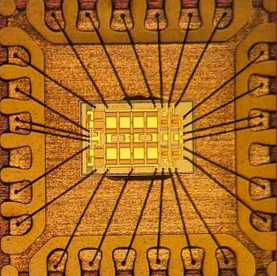 QFN Series
AVG1012
QFN RF / power module
4mm × 4mm
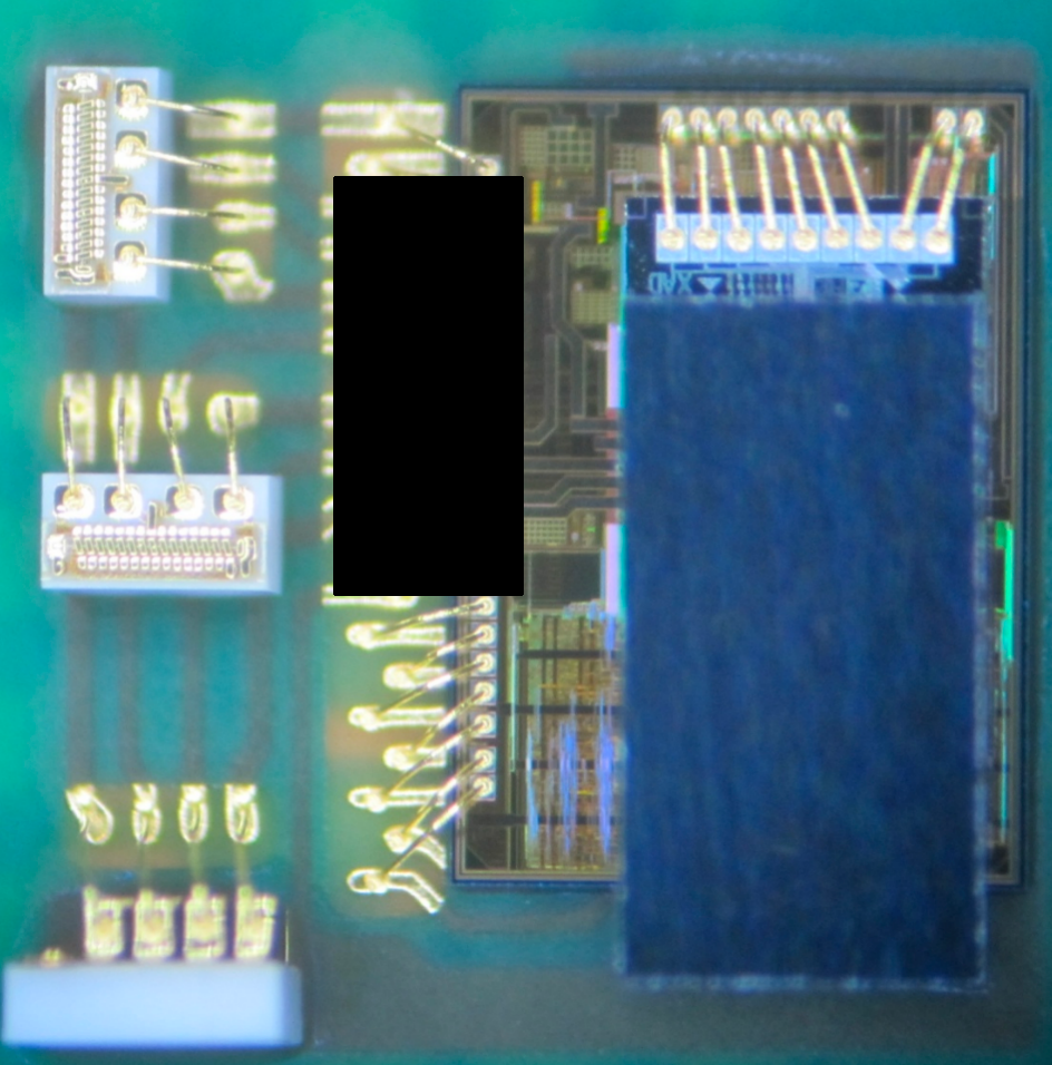 LGA 6 axis / 2.5D
6-Axis Gyroscope (AMI603)
MEMS application · SiP packaging
3mm × 3mm
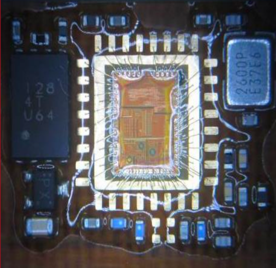 SiP Module
SiP System-in-Package
High integration · multi-chip synergy
10mm × 13mm
Certifications & Compliance
Certified to multiple international systems, with full process traceability
ISO 9001:2015
Quality Management System
ISO 14001:2015
Environmental Management System
IATF 16949:2016
Automotive Quality Management System